

Molybdenum Microhole Plates
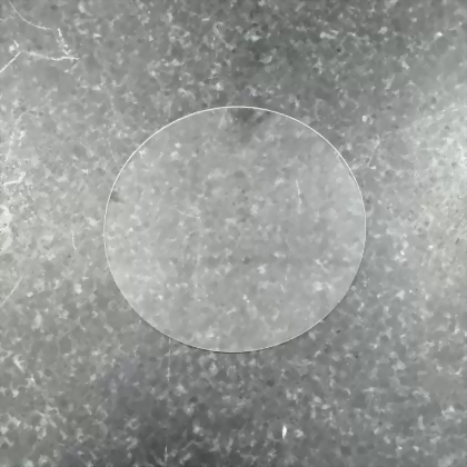
Hortech performs laser micro-drilling on 50 μm-thick molybdenum sheets to manufacture precision microhole components for advanced electron beam applications.
Over the next two decades, the evolution of Moore’s Law is expected to follow two major trends. The first is the continued scaling of lithography density, which demands increasingly higher resolution in inspection and metrology systems. The second is the growing adoption of 2.5D and 3D scaling technologies, which require inspection systems capable of handling structures with extremely high aspect ratios.
In electron beam inspection systems, the electron gun emits an electron beam, which is accelerated by the anode. Focusing optics align and calibrate the beam, while the objective lens focuses it onto the sample surface. Defect scanning coils raster the focused beam across the sample, and detectors collect emitted signals from the sample surface. The imaging system synchronizes these signals with the scanning position to generate high-resolution inspection images.
Electron beam technology can be applied to:
-
Metrology and measurement
-
Voltage contrast defect inspection
-
Physical defect inspection
E-beam inspection provides ultra-high resolution, high defect capture rates, and highly stable performance. Wafer defects must be identified and eliminated to improve die yield, and electron beam inspection is capable of detecting defects that conventional optical inspection systems cannot identify.
Electron beam systems can inspect wafer surfaces and defects embedded within complex 3D structures across a broad range of landing energies while maintaining extremely high resolution. In addition, electron beam voltage contrast inspection remains one of the few practical methods capable of detecting voltage-related defects.
Within an electron beam inspection system, the generated electron beam strikes the wafer surface and interacts with the material. Scattered electrons are collected by detectors to identify defects. Compared with optical inspection systems, electron beam inspection offers significantly higher sensitivity and can reveal defects beyond the detection capability of optical methods.
Electron beam systems typically generate two types of electron signals:
-
Secondary Electrons (SE): Low-energy electrons emitted from the sample surface, providing detailed surface information.
-
Backscattered Electrons (BSE): Higher-energy electrons that penetrate deeper into the sample structure.
Key system requirements include:
-
High Vacuum Environment — allowing electrons to travel without interference.
-
High Voltage Acceleration — attracting and accelerating electrons from the source to ensure stable beam generation and inspection performance.
#Laser Micro-Drilling #Optical Filtering Devices #Optical Conversion Devices #Microholes #Miniature Holes #Electron Microscope Consumables #Critical Electron Beam Components #Electron Beam Aperture Plates #E-Beam Inspection #eBeam
- Electron Microscope Components
- Inspection Equipment
- Critical Components
- Microholes
- Molybdenum Sheets
- Electron Beam Lithography Consumables
Laser micro-drilling on 50 μm-thick molybdenum sheets is used to manufacture critical components for electron microscopes. Hortech can provide precision drilling solutions with customized hole dimensions and depths based on customer requirements, applicable to metals as well as thin, brittle, and high-hardness materials for critical inspection and metrology equipment components.